
Why POM-TAG exists
There was no shortage of JTAG programmers when I started POM-TAG. Buying one would have been the sensible option. It would also have meant treating another part of the FPGA toolchain as a finished black box.
I wanted to understand what actually happens between Vivado Hardware Manager and the FPGA: how an FTDI device is identified by Vivado, how its EEPROM is configured, how the MPSSE generates the JTAG transactions, and how those signals are presented safely to a target that may not use 3.3 V logic. POM-TAG became a small project built around that interface rather than around the FPGA itself.
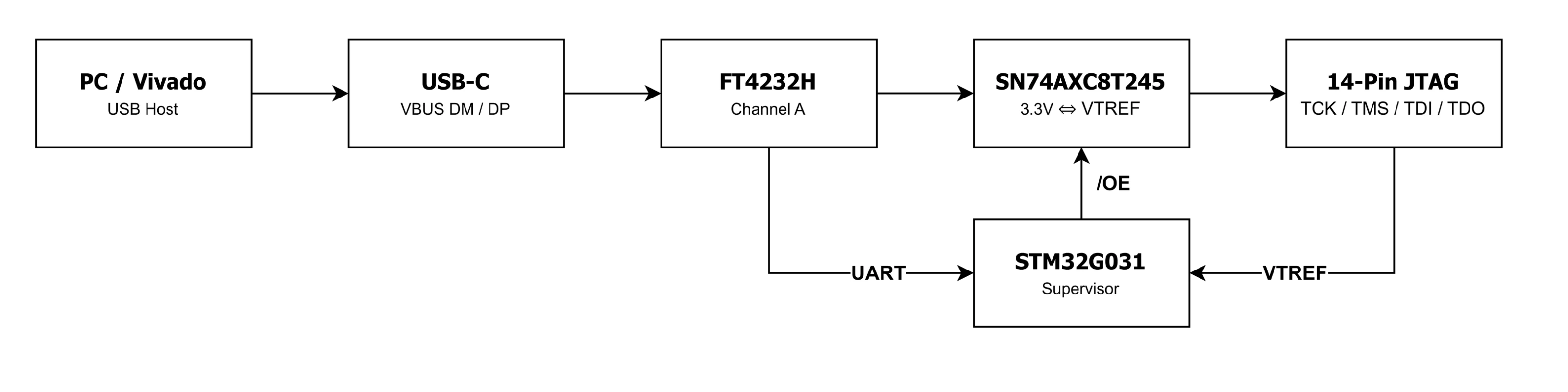
The hardware therefore goes further than a basic FT4232H breakout. The FT4232H handles USB and generates the JTAG signals, but the target side is level-shifted through an SN74AXC8T245 level translator. VTREF is taken from the FPGA board and used to set the target-side logic level, allowing the same programmer to work with JTAG banks operating at 1.5 V, 1.8 V, 2.5 V or 3.3 V. An STM32 measures that reference voltage and keeps the translator disabled until the target voltage is valid. If the target is disconnected or powered down, the JTAG outputs return to a high-impedance state.
I also wanted the programmer to expose more information than a single power LED. The STM32 controls an RGB LED that reports VTREF validity, JTAG activity, device detection, programming progress and the final result. Vivado-related events are sent to the MCU through one of the spare FT4232H UART channels, while the JTAG timing itself remains entirely inside the FTDI hardware.
The result is not an attempt to replace commercial programming cables. POM-TAG is a programmer built to make the interface understandable, measurable and reusable as part of the wider Pomsera FPGA work. And yes, building a programmer because programmers already exist is slightly backwards. That was also part of the appeal.
Xilinx 14-pin JTAG header
The interactive diagram below explains the standard Xilinx 14-pin JTAG header, showing the function of each pin and the placement of TCK, TMS, TDI, TDO, VTREF, ground and the optional reset signals.
POM-TAG Hardware Architecture
| Function | Implementation |
|---|---|
| Host connection | USB-C |
| USB/JTAG controller | FTDI FT4232H |
| JTAG engine | Channel A in MPSSE mode |
| Configuration memory | Microchip AT93C56B, 2-Kbit Microwire EEPROM |
| Supervisor | STM32G031K8U |
| Level translator | TI SN74AXC8T245RHLR |
| Supported target reference | 1.5 V to 3.6 V |
| Target signals | TCK, TMS, TDI, TDO and VTREF |
| Target reset | SRST not supported |
| Target connector | 14-pin, 2 x 7 Xilinx-style JTAG header |
| Target power | Not supplied by POM-TAG |
| Status | Common-anode RGB LED driven by the STM32 |
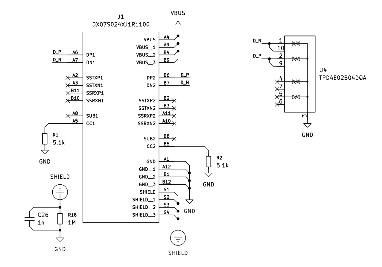
USB-C input and the 3.3 V supply
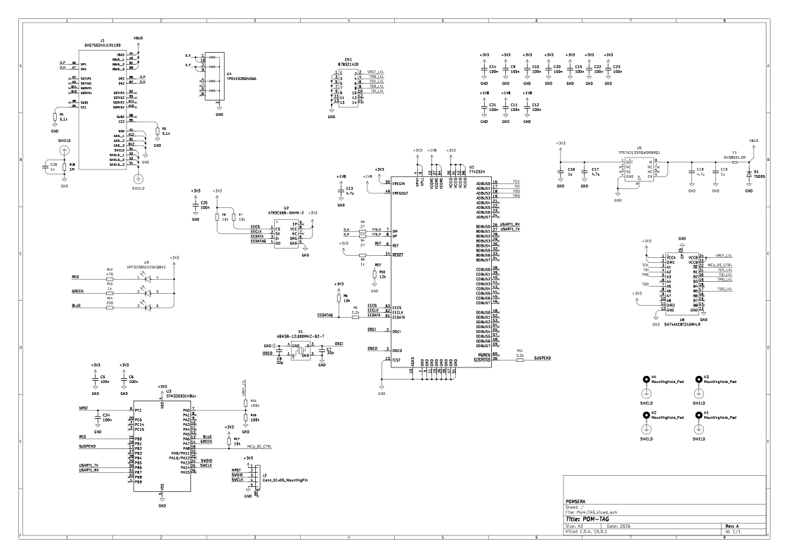
The USB-C connector provides both the data connection and the 5 V bus supply. POM-TAG is a USB
device, so CC1 and CC2 each use a 5.1 kΩ pull-down resistor. The duplicated USB 2.0 D+ pins are tied
together, as are the duplicated D- pins, which preserves the data pair regardless of plug orientation.
D+ and D- pass through a low-capacitance ESD protection device before reaching the FT4232H. The
FTDI-side USB inputs include the 27 Ω series resistors shown in the schematic. These parts belong close to
the USB signal path because their purpose is electrical, not logical: the ESD array limits transient stress at
the connector, while the series resistors control the edge presented to the FTDI pins.
The connector shell is not shorted directly to logic ground in the schematic. A 1 nF capacitor and a 1 MΩ resistor connect the shield to ground in parallel. The capacitor provides a high-frequency return path while the resistor prevents the shield from remaining indefinitely floating at DC.
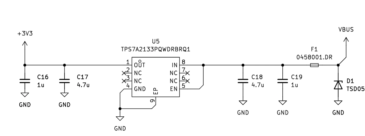
VBUS is protected before it is converted to the board's 3.3 V rail. The input network contains the VBUS transient suppressor, the series protection element and local input capacitance. U5 is the fixed 3.3 V regulator for the programmer electronics. Its output feeds the STM32, EEPROM, FT4232H I/O domains and the A side of the JTAG translator.
FT4232H power domains
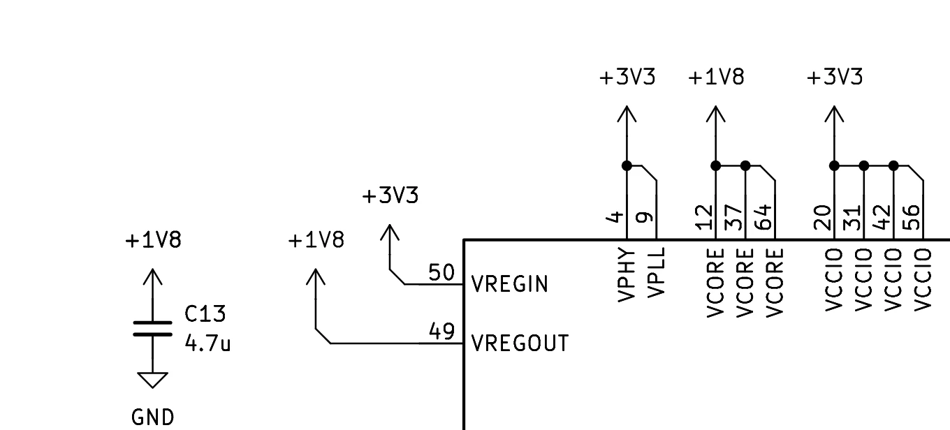
The FT4232H itself uses both 3.3 V and 1.8 V. VREGIN is connected to 3.3 V, and the device's internal regulator produces the 1.8 V VREGOUT rail used by the FTDI core. The 4.7 µF capacitor on VREGOUT is part of that regulator implementation. VPHY, VPLL and the selected VCCIO pins remain on the 3.3 V rail in this design. Keeping these domains explicit in the schematic is useful during bring-up: a board can have a valid 3.3 V supply and still fail if the FTDI core rail is absent.
FT4232H: USB interface and JTAG engine
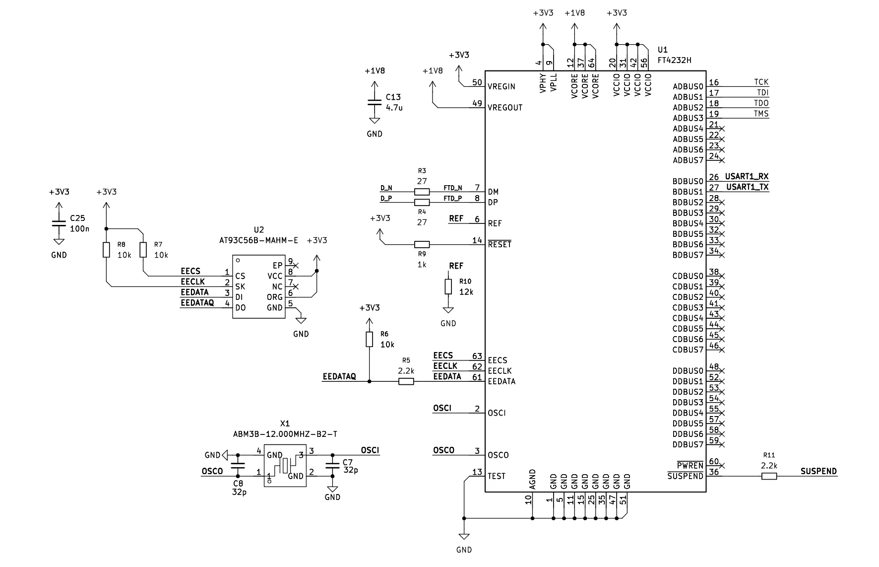
Channel A of the FT4232H is dedicated to JTAG. The important connection is not simply that four GPIO pins reach the header; the device uses its Multi-Protocol Synchronous Serial Engine, or MPSSE, to generate the clocked JTAG transaction in hardware. Vivado sends command blocks over USB and the MPSSE executes the corresponding TCK, TMS and data sequence locally. The spacing of individual JTAG edges is therefore not determined by USB packet latency.
| Function | Implementation |
|---|---|
| ADBUS0 | TCK - clock generated by the FT4232H |
| ADBUS1 | TDI - data from POM-TAG to the target |
| ADBUS2 | TDO - data returned by the target |
| ADBUS3 | TMS - TAP state control |
The 12 MHz crystal is connected directly to OSCI and OSCO. Its two load capacitors return to ground. On the PCB, the crystal and its load network should remain close to the FT4232H, with short traces and a clean return path. The same placement rule applies to the local decoupling capacitors around VPLL, VPHY, VCORE and VCCIO.
EEPROM configuration and the current program_ftdi workflow
The AT93C56B stores the non-volatile FTDI configuration read during USB enumeration. This step is required for Vivado Hardware Manager to recognise the FT4232H as a supported USB-to-JTAG cable. AMD documents the procedure in UG908 and provides the program_ftdi utility with the Vivado installation. For a POM-TAG development unit, the EEPROM can be written with the following command:
1program_ftdi -write -ftdi FT4232H -serial POM00001 -vendor "Pomsera" -board "POM TAG" -desc "USB-JTAG programmer"The programmed contents can then be read back:
1program_ftdi -readAfter the EEPROM has been written, disconnect and reconnect USB so that the FT4232H enumerates again with the new contents. AMD's utility assigns Channel A to USB-JTAG. On an FT4232H, the remaining channels are left in their default UART mode unless they are reconfigured separately. The Manufacturer field is a special case. AMD states that program_ftdi sets it to Xilinx and that changing this field prevents Vivado from recognising the device as a USB-to-JTAG cable. POM-TAG identification therefore belongs in the Vendor, Board, Description and Serial fields, while the Manufacturer field is left as required by AMD.
Translating JTAG to the target voltage
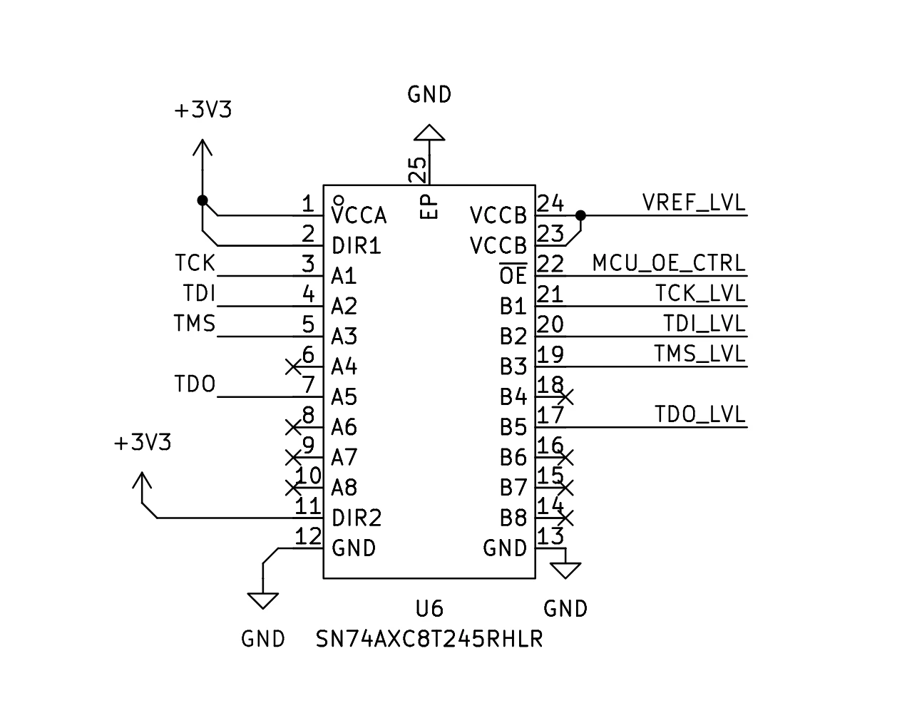
The FT4232H side of the interface operates at 3.3 V, but the target JTAG bank may not. POM-TAG uses an SN74AXC8T245 so the programmer can keep its own 3.3 V domain while adopting the voltage supplied by the target on VTREF. VCCA is tied to 3.3 V. Both VCCB pins are tied to VREF_LVL, the target-derived reference voltage.
The translator is arranged so that the JTAG directions are fixed in hardware. TCK, TDI and TMS occupy channels 1 to 3 and travel from the A bus to the B bus. TDO occupies channel 5 and travels from the B bus back to the A bus. DIR1 and DIR2 are both tied high. According to the SN74AXC8T245 function table, that combination produces A-to-B transfer on bits 1 to 4 and B-to-A transfer on bits 5 to 8 when OE is low. No firmware is required to reverse the data direction during a scan.
| Function | Implementation |
|---|---|
| TCK | A1 → B1, programmer to target |
| TDI | A2 → B2, programmer to target |
| TMS | A3 → B3, programmer to target |
| TDO | B5 → A5, target to programmer |
| VCCA | 3.3 V from POM-TAG |
| VCCB | VREF_LVL from the target |
| DIR1 / DIR 2 | Both high: bits 1-4 A → B, bits 5-8 B → A |
| OE | Active low, controlled by the STM32 |
Texas Instruments specifies both voltage domains of the SN74AXC8T245 for 0.65 V to 3.6 V operation. POM-TAG deliberately specifies a narrower 1.5 V to 3.6 V target range because that is the range validated for the intended FPGA use. A 5 V target reference is not supported and must not be connected to VREF_LVL.
VTREF supervision and safe output enable
VTREF performs two jobs. Electrically, it powers VCCB of the SN74AXC8T245 and therefore defines the
logic-high level presented to the target. Independently, the same voltage is measured by the STM32
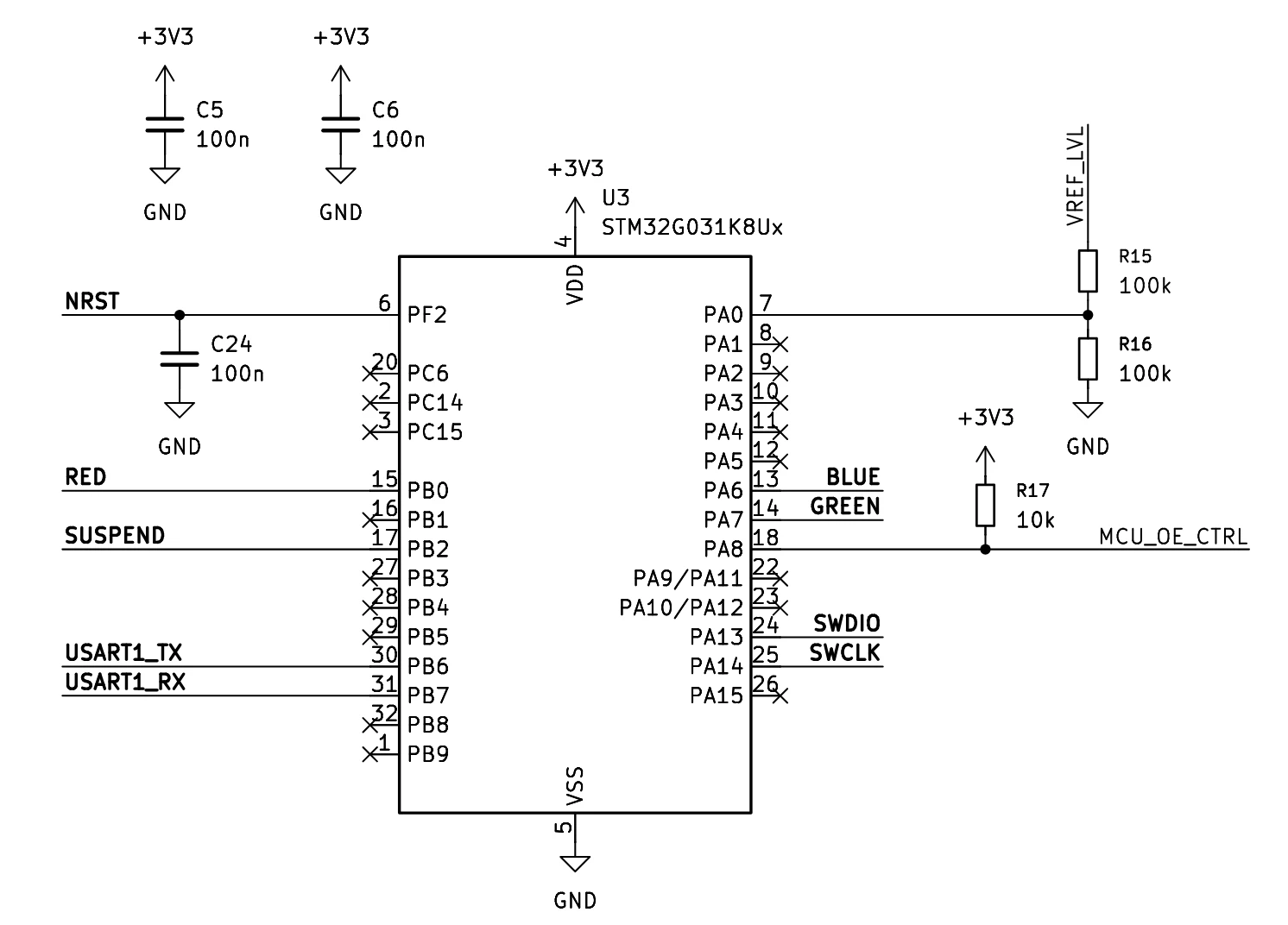
through a 100 kΩ / 100 kΩ divider connected to PA0. The target is not powered from VTREF; the pin is only
a reference and a light load for the translator and ADC divider.
With equal resistor values, the ADC sees half of the target reference voltage: VADC = VTREF / 2. A 1.8 V
target therefore produces about 0.90 V at PA0, while a 3.3 V target produces about 1.65 V. The divider's
Thevenin resistance is approximately 50 kΩ, so the ADC must be configured with enough sampling time for
its internal sample-and-hold capacitor to settle. Averaging in firmware prevent noise around
the acceptance threshold from repeatedly enabling and disabling the interface.
| Function | Implementation |
|---|---|
| 1.5V VTREF | 0.75V at PA0 |
| 1.8V VTREF | 0.90V at PA0 |
| 2.5V VTREF | 1.25V at PA0 |
| 3.3V VTREF | 1.65V at PA0 |
| 3.6V VTREF | 1.80V at PA0 |
The translator's OE input is active low. MCU_OE_CTRL is pulled up to 3.3 V, which leaves the translator
disabled while the STM32 is in reset or its GPIO is still unconfigured. Only after firmware has measured a stable VTREF inside the supported range does the MCU drive OE low. If VTREF disappears, the interface is
disabled again.
This arrangement prevents the FT4232H from actively driving TCK, TMS or TDI into an unpowered target.
It also makes the safety decision independent of the Vivado status script. UART messages can change the
LED state, but they do not authorise the JTAG outputs. The translator's own VCC isolation and partial power-down behaviour provide an additional device-level safeguard when one voltage domain is absent.
Target connector and the SRST limitation
CN1 is a 2 x 7 Xilinx-style JTAG header. The implemented signal pins are VREF_LVL, TMS_LVL, TCK_LVL,
TDO_LVL and TDI_LVL. The odd-numbered positions in the schematic are used as ground returns, while
pins 12 and 14 are left unconnected. POM-TAG does not supply a target power rail through this connector;
the FPGA board must already be powered and must provide VTREF.
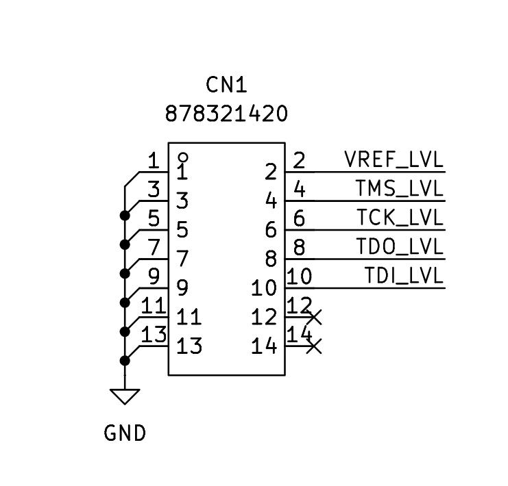
The number of ground contacts is intentional. JTAG is a digital protocol, but the cable still carries fast edges. A low nominal TCK frequency does not imply low-frequency signal behaviour. Short return paths beside the active signals reduce loop area and help preserve the TCK waveform at the target connector.
STM32 supervision, UART status and the RGB LED
The STM32G031K8U is a supervisor, not a second JTAG controller. Its direct hardware responsibilities are
limited to measuring VTREF, controlling MCU_OE_CTRL and driving the status LED. The FTDI SUSPEND
signal is also routed to the MCU, which gives the firmware visibility of the USB-side state if required.
SWDIO, SWCLK and NRST are broken out on the local service header so the supervisor firmware can be
programmed independently.
A spare FT4232H channel provides the status link between the host and the supervisor. On Channel B,
BDBUS0 is the FTDI transmit signal and is connected to the MCU's USART1_RX net; BDBUS1 is the FTDI
receive signal and is connected to USART1_TX. A companion Vivado Tcl script can therefore send short
status messages to the STM32 without interfering with Channel A, which remains dedicated to MPSSE
JTAG.
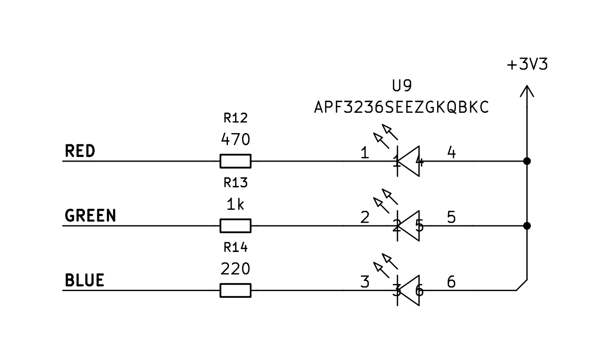
The RGB LED is common-anode and tied to 3.3 V. The STM32 sinks current through separate resistors for the red, green and blue dies. The resistor values differ because the three LED dies have different forward voltages and luminous efficiencies. The LED is therefore a hardware output driven by firmware, not an indication produced by the FTDI device itself.
PCB implementation
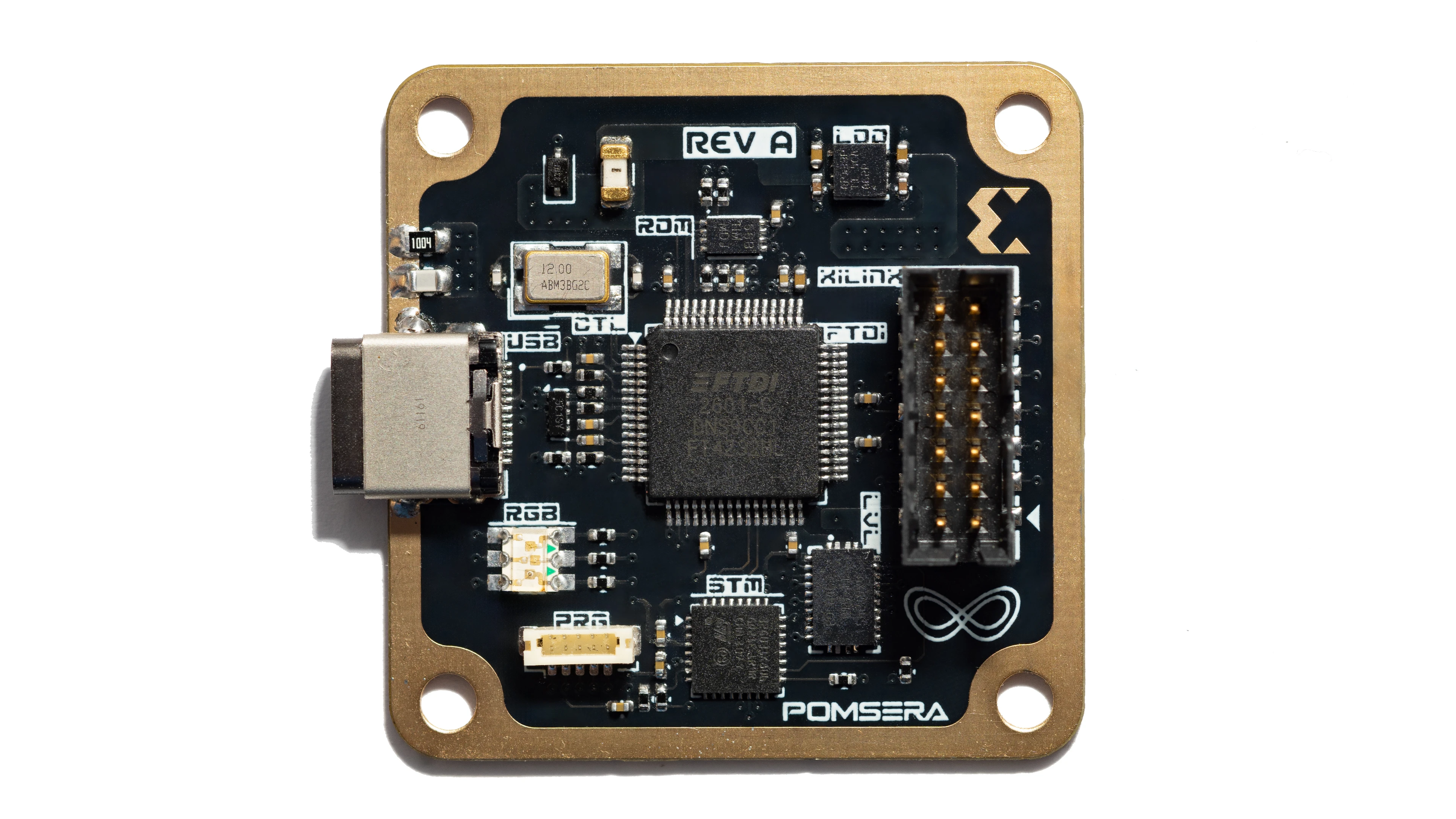
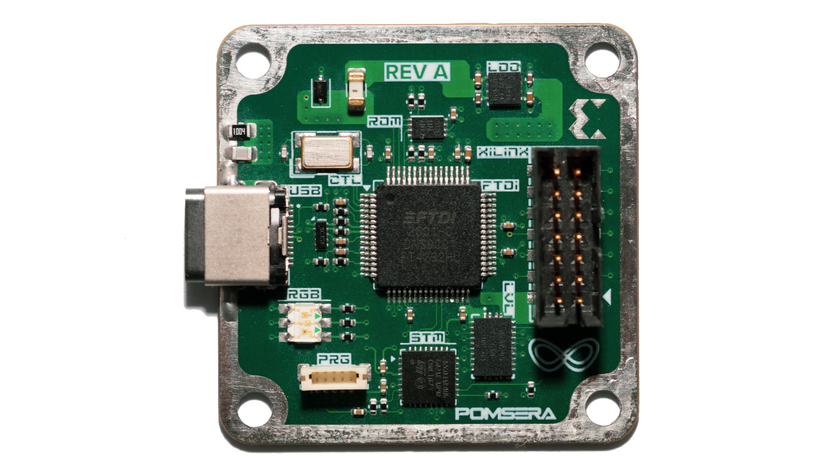
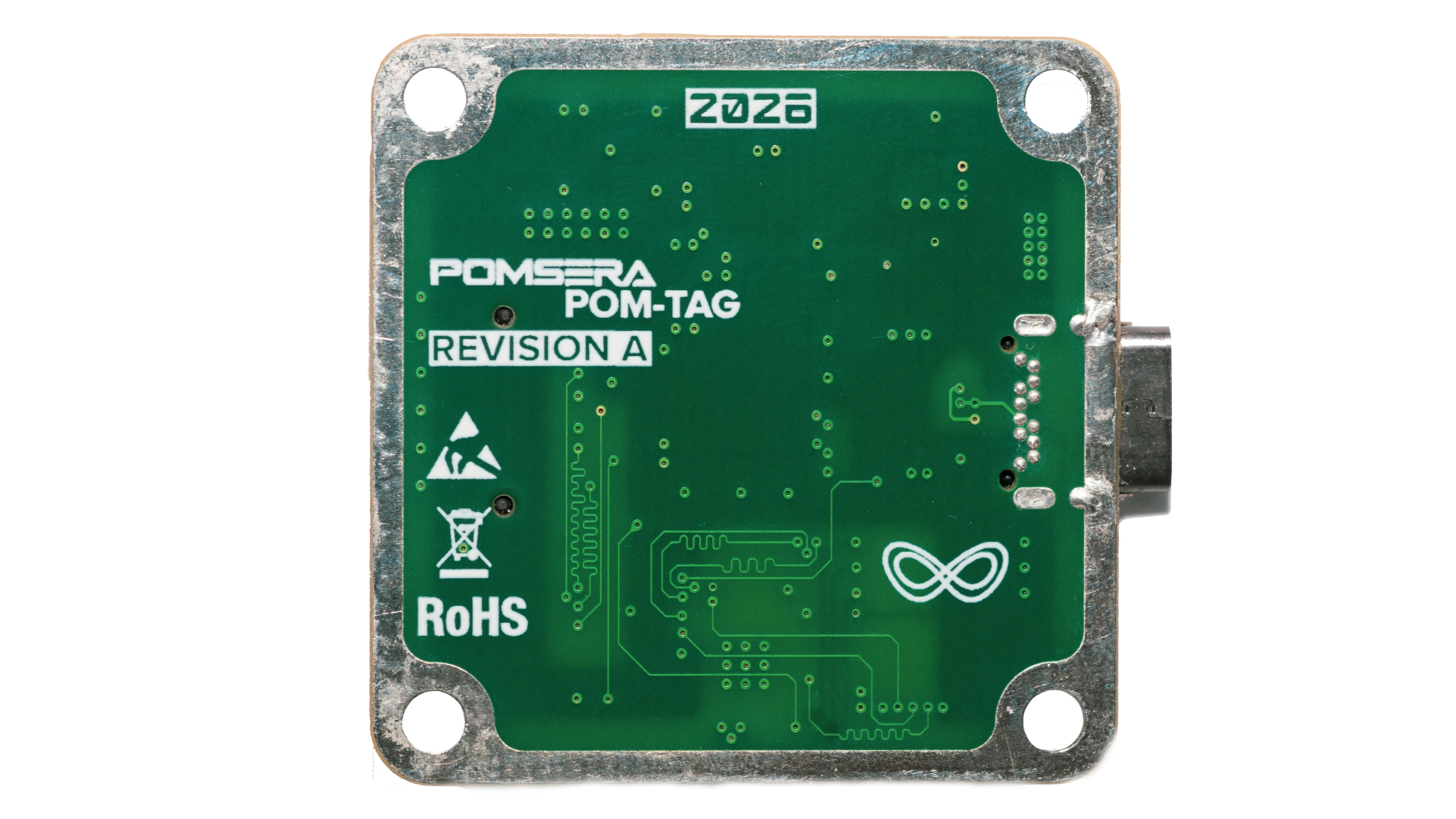
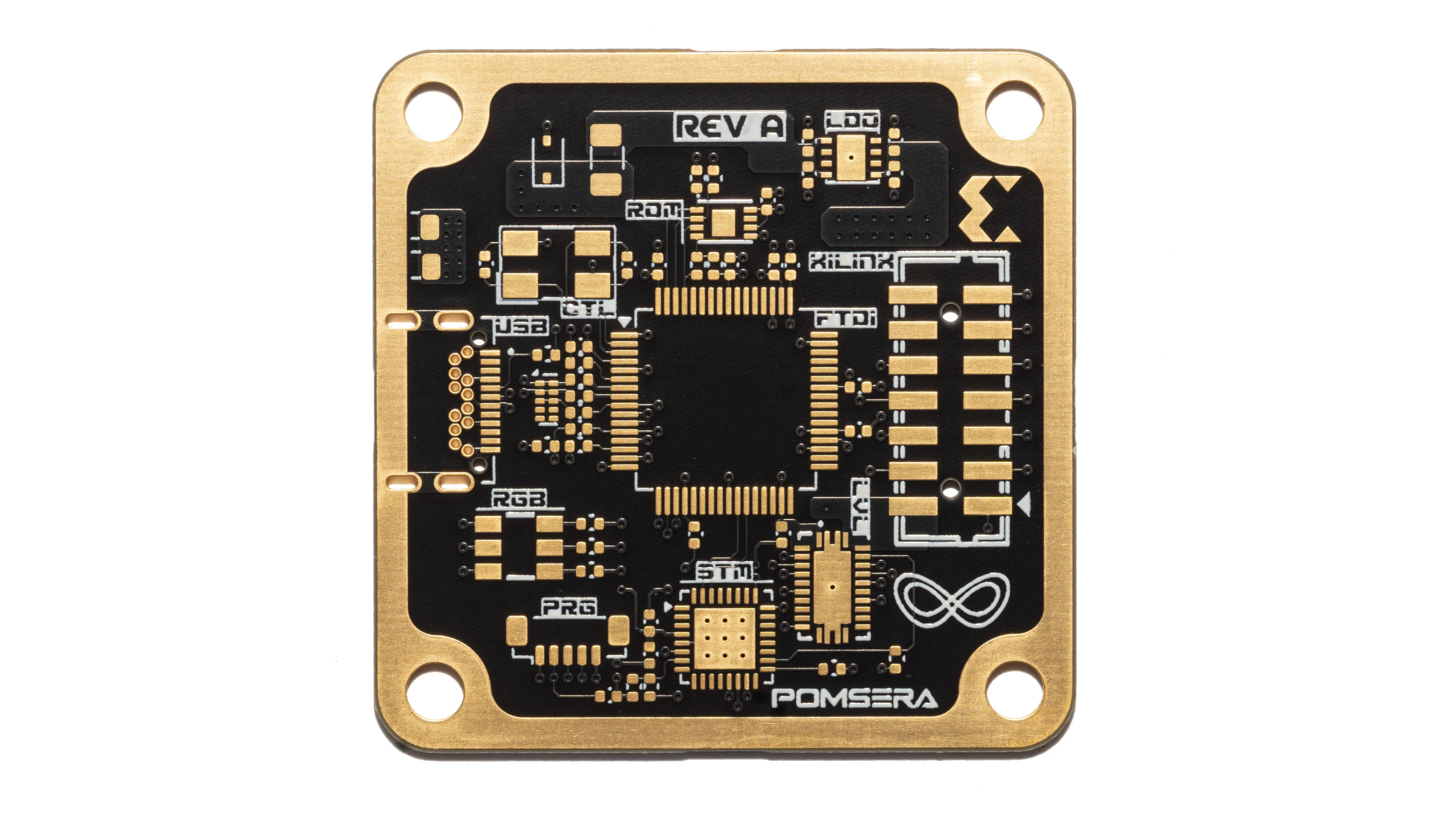
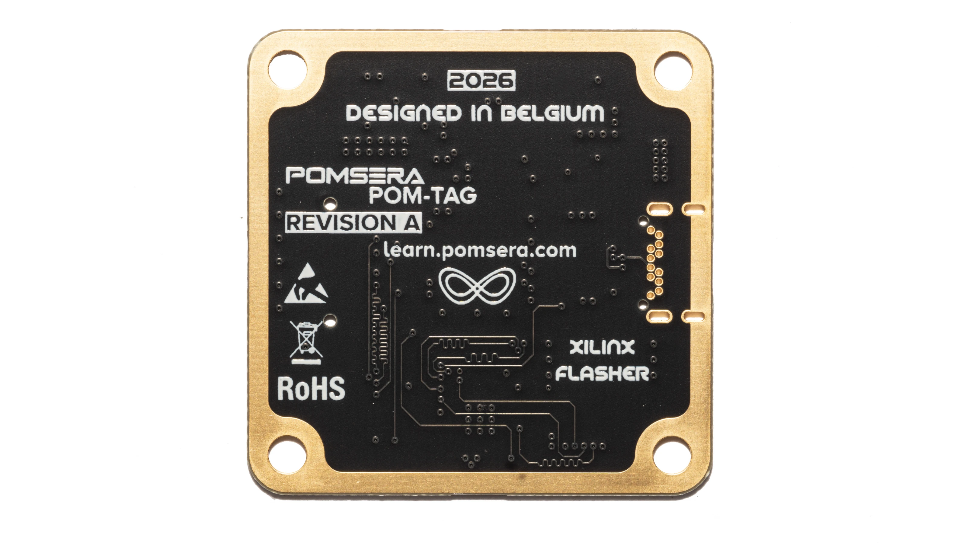
The POM-TAG PCB brings the complete programmer into a single compact board. The USB-C interface and input protection form the host-side connection, while the FT4232H sits at the centre of the design as the main USB-to-JTAG controller. Its configuration EEPROM and 12 MHz crystal are placed around the FTDI device as part of the same functional block. The SN74AXC8T245 separates the FTDI’s 3.3 V logic domain from the target JTAG voltage and connects directly to the 2 × 7 programming header. The STM32G031 is kept outside the JTAG timing path and handles VTREF supervision, translator enable control and the RGB status LED. Power regulation and decoupling complete the board, providing the 3.3 V rail used by the digital logic and the 1.8 V core supply required by the FT4232H. The result is a PCB where USB communication, JTAG generation, voltage translation and supervision remain separate functions, but operate together as a single programmer.
Documentation
Schematic
Printed Circuit Board

Best viewed on a computer
The Gerber viewer is interactive and only displays on a larger screen.

Inspect this board's Gerber layers in 2D and 3D. Loads on demand to keep the page fast.

3D Case
Best viewed on a computer
The STL viewer is interactive and only displays on a larger screen.
Best viewed on a computer
The STL viewer is interactive and only displays on a larger screen.
Digilent JTAG Adapter for Single-Row Headers
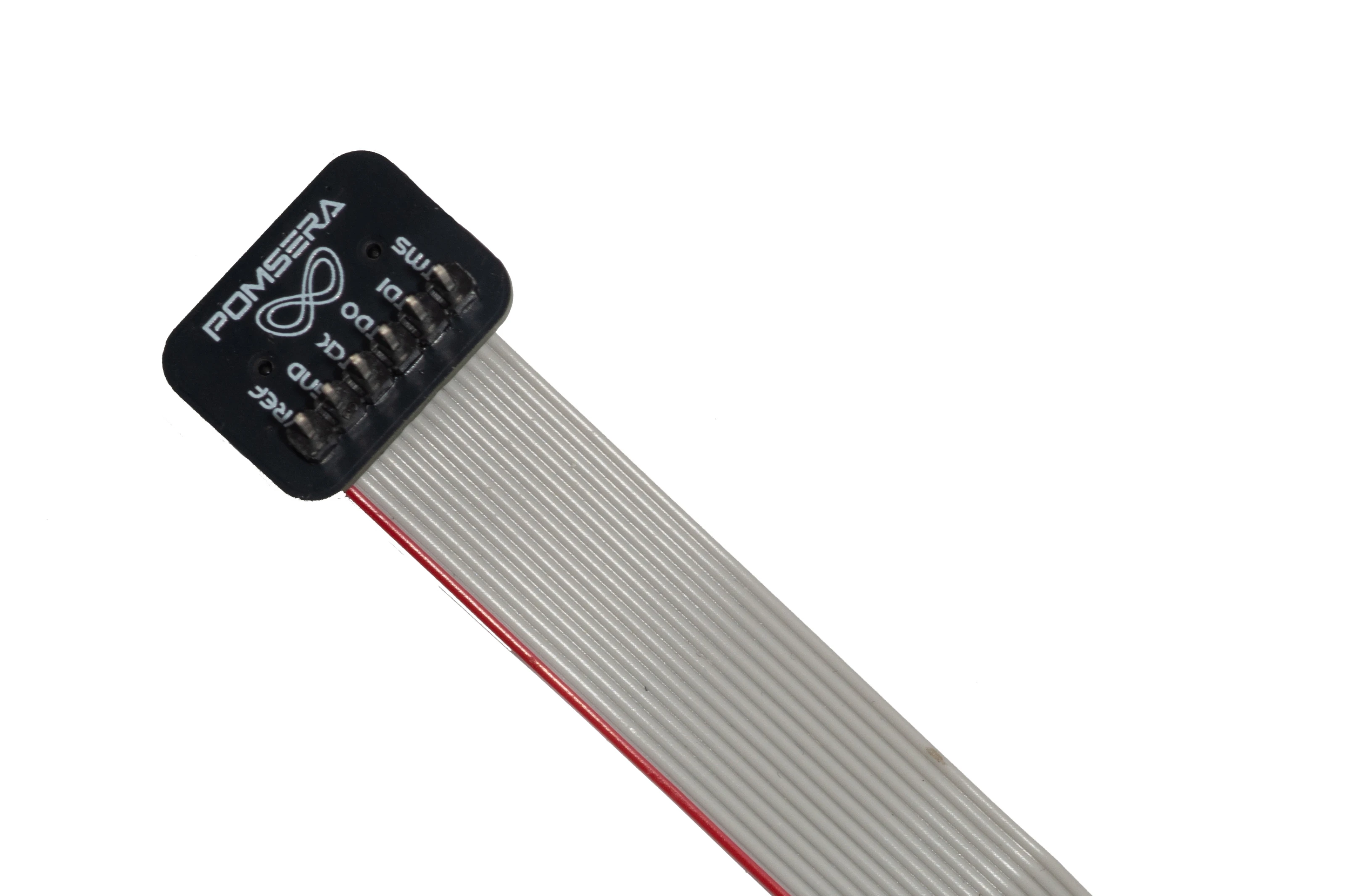
Since some of the boards I use expose Digilent’s single-row JTAG footprint rather than the standard Xilinx 2 × 7 header, I made a small adapter for POM-TAG as well. It remaps TCK, TMS, TDI, TDO, VTREF and ground between the two connector formats, so the same programmer can be used without modifying the target board or the POM-TAG hardware.
Best viewed on a computer
The Gerber viewer is interactive and only displays on a larger screen.
Inspect this board's Gerber layers in 2D and 3D. Loads on demand to keep the page fast.
Test With Arty S7-50

Video available in the online article.
Firmware
STM32 supervision
The FT4232H handles the JTAG timing, while the STM32 supervises the target voltage, controls the level translator and drives the status LED. The relevant pin definitions are:
1#define VTREF_SENSE PA02#define JTAG_OE PA834#define FT_RX PB75#define FT_TX PB6Measuring VTREF
The firmware averages 64 ADC samples and compensates for the 2:1 divider:
1float readVTREF()2{3 uint32_t total = 0;45 for (int i = 0; i < 64; i++)6 total += analogRead(VTREF_SENSE);78 float raw = total / 64.0f;910 float pinVoltage =11 (raw / 4095.0f) * 3.3f;1213 return pinVoltage * 2.0f;14}This gives the STM32 an estimate of the actual voltage present on the target VTREF pin.
Enabling the JTAG interface
The translator always starts disabled:
1pinMode(JTAG_OE, OUTPUT);2digitalWrite(JTAG_OE, HIGH);OE is active low, so HIGH places the JTAG translator outputs in high impedance.
When VTREF becomes valid, it must remain stable for 600 ms before JTAG is enabled:
1if (!targetValid && vtrefCandidate)2{3 if (millis() - vtrefCandidateSince >= 600)4 {5 targetValid = true;6 digitalWrite(JTAG_OE, LOW);7 }8}If VTREF becomes invalid, the translator is disabled immediately:
1if (!measurementValid)2{3 digitalWrite(JTAG_OE, HIGH);4}The delayed enable prevents a transient voltage from activating the interface, while loss of target power disconnects the JTAG outputs without waiting for the LED state to change.
Vivado status over UART
A spare FT4232H channel connects Vivado to the STM32 at 115200 baud:
1FTSerial.begin(115200);The protocol is deliberately small:
1H heartbeat2I idle3C connecting4B FPGA detected / JTAG ready5S scan6P programming7V verify8D success9E errorThe companion Tcl script sends these characters as Vivado moves through the programming sequence. The MCU converts them into LED states.
For example:
1if (c == 'P')2 requestVivadoState(VIVADO_PROGRAM);34if (c == 'D')5 resultEvent = RESULT_SUCCESS;67if (c == 'E')8 resultEvent = RESULT_ERROR;The UART is not part of the safety path. Losing the Vivado connection only clears the displayed software state; VTREF supervision continues independently.
LED states
The RGB LED gives a quick indication of both hardware and Vivado state:
| State | LED |
|---|---|
| Invalid VTREF | Slow orange pulse |
| Valid VTREF | Yellow |
| Connecting | Blue/cyan pulse |
| FPGA detected | Double cyan flash |
| JTAG ready | Cyan breathing |
| Scan | Fast blue |
| Programming | Violet strobe |
| Verify | Amber |
| Success | Green |
| Error | Red |
Download

Software
Installing the Vivado integration
POM-TAG uses two Tcl files. The first is the actual integration script, pomsera_vivado.tcl. The second is a very small Vivado startup file whose only job is to load it automatically.
With the files provided here, the expected Windows layout is:
1C:\2└── Pomsera\3 └── pomsera_vivado.tcl45%APPDATA%\6└── Xilinx\7 └── Vivado\8 └── Vivado_init.tclAMD Vivado automatically looks for Vivado_init.tcl in the user's Vivado configuration directory when it starts.
1%APPDATA%\Xilinx\Vivado\2025.2\Vivado_init.tclThat path is already present in the supplied Vivado_init.tcl, so placing the main script in C:\Pomsera\pomsera_vivado.tcl requires no modification.
The sequence at startup is therefore:
1Vivado starts2 │3 ▼4Vivado_init.tcl5 │6 ▼7C:\Pomsera\pomsera_vivado.tcl8 │9 ├── detect POM-TAG COM ports10 ├── open the UART connection11 ├── watch Vivado journal/log events12 └── monitor the connected FPGAThe main script initializes itself after being loaded, opens the serial interface when available, attaches to the current Vivado session files and starts its background watchers.
If the script is edited while Vivado is already open, it does not need to be restarted. The integration provides:
1::pomsera::reloadwhich cleanly stops the existing instance and reloads the same file.
Download

BOM

Key non-passive components:
| Qty | Part | Where to buy |
|---|---|---|
| 1 | 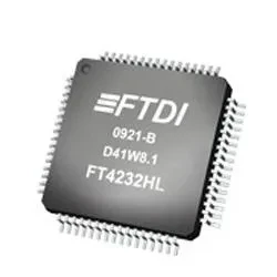 FT4232HL-REELUSB Bridge, USB to UART USB 2.0 UART Interface 64-LQFP (10x10) |  DigiKeyBuy  MouserBuy  LCSCBuy |
| 1 |  AT93C56B-MAHM-EEEPROM Memory IC 2Kbit 3-Wire Serial 2 MHz 8-UDFN (2x3) | DigiKeyBuy MouserBuy LCSCBuy |
| 1 |  STM32G031K8U6ARM® Cortex®-M0+ STM32G0 Microcontroller IC 32-Bit 64MHz 64KB (64K x 8) FLASH 32-UFQFPN (5x5) | DigiKeyBuy MouserBuy LCSCBuy |
| 1 |  TPD4E02B04DQA8.8V (Typ) Clamp 5A (8/20µs) Ipp Tvs Diode Surface Mount 10-USON (2.5x1) | DigiKeyBuy MouserBuy LCSCBuy |
| 1 | 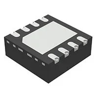 TPS7A2133PQWDRBRQ1Linear Voltage Regulator IC Positive Fixed 1 Output 500mA 8-SON (3x3) | DigiKeyBuy MouserBuy LCSCBuy |
| 1 | 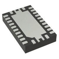 SN74AXC8T245RHLRTranslation Transceiver 1 Element 8 Bit per Element Tri-State, Non-Inverted Output 24-VQFN (5.5x3.5) | DigiKeyBuy MouserBuy LCSCBuy |
| 1 | 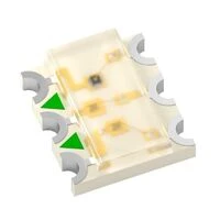 APF3236SEEZGKQBKCMulti-Colour LEDs 3.2x3.6MM RGB SM RGB SMD | DigiKeyBuy MouserBuy LCSCBuy |
| 1 | 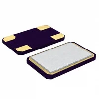 ABM3B-12.000MHZ-B2-T12 MHz ±20ppm Crystal 18pF 70 Ohms 4-SMD, No Lead | DigiKeyBuy MouserBuy LCSCBuy |
| 1 | 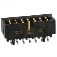 0878321420Connector Header Surface Mount 14 position 0.079" (2.00mm) | DigiKeyBuy MouserBuy LCSCBuy |
| 1 | 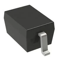 TSD05DYFR9V (Typ) Clamp 60A (8/20µs) Ipp Tvs Diode Surface Mount SOD-323 | DigiKeyBuy MouserBuy LCSCBuy |
| 1 | 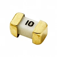 0458001.DRSurface Mount Fuses 48VAC 1A .18ohms 458 NANO2 | DigiKeyBuy MouserBuy LCSCBuy |
| 1 | 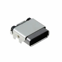 DX07S024XJ1R1100USB Connectors HYBRID SMT/THRU-HOLE STD MNT - USB TYPE | DigiKeyBuy MouserBuy LCSCBuy |
| 1 |  BM05B-SURS-TFCONN HEADER SMD 5POS 0.8MM | DigiKeyBuy MouserBuy LCSCBuy |
| 13 | 13 lines | |