
Introduction
Most oscilloscopes are designed to show voltage against time. PomScope Mini was designed to plot state variables against one another.
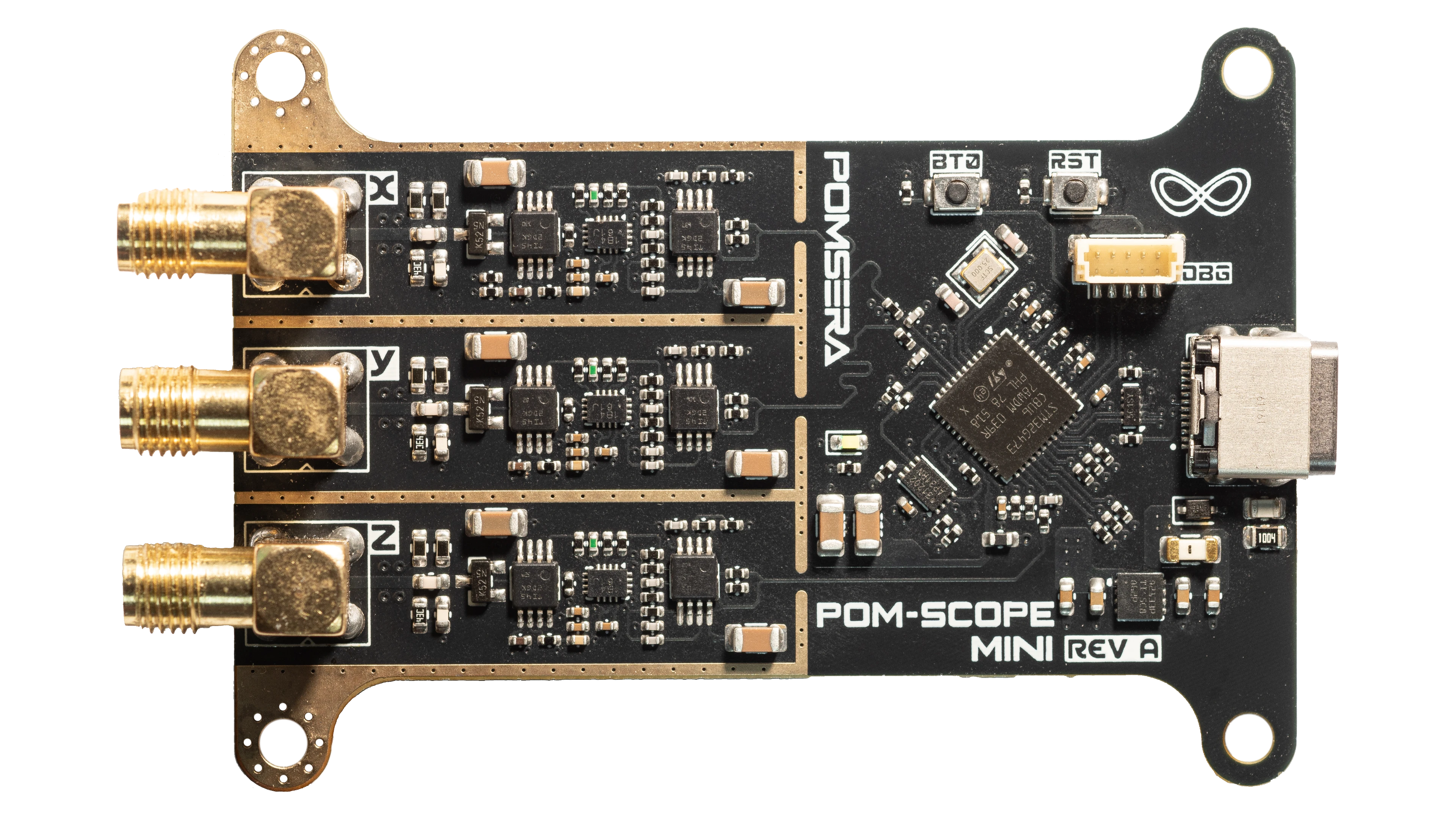
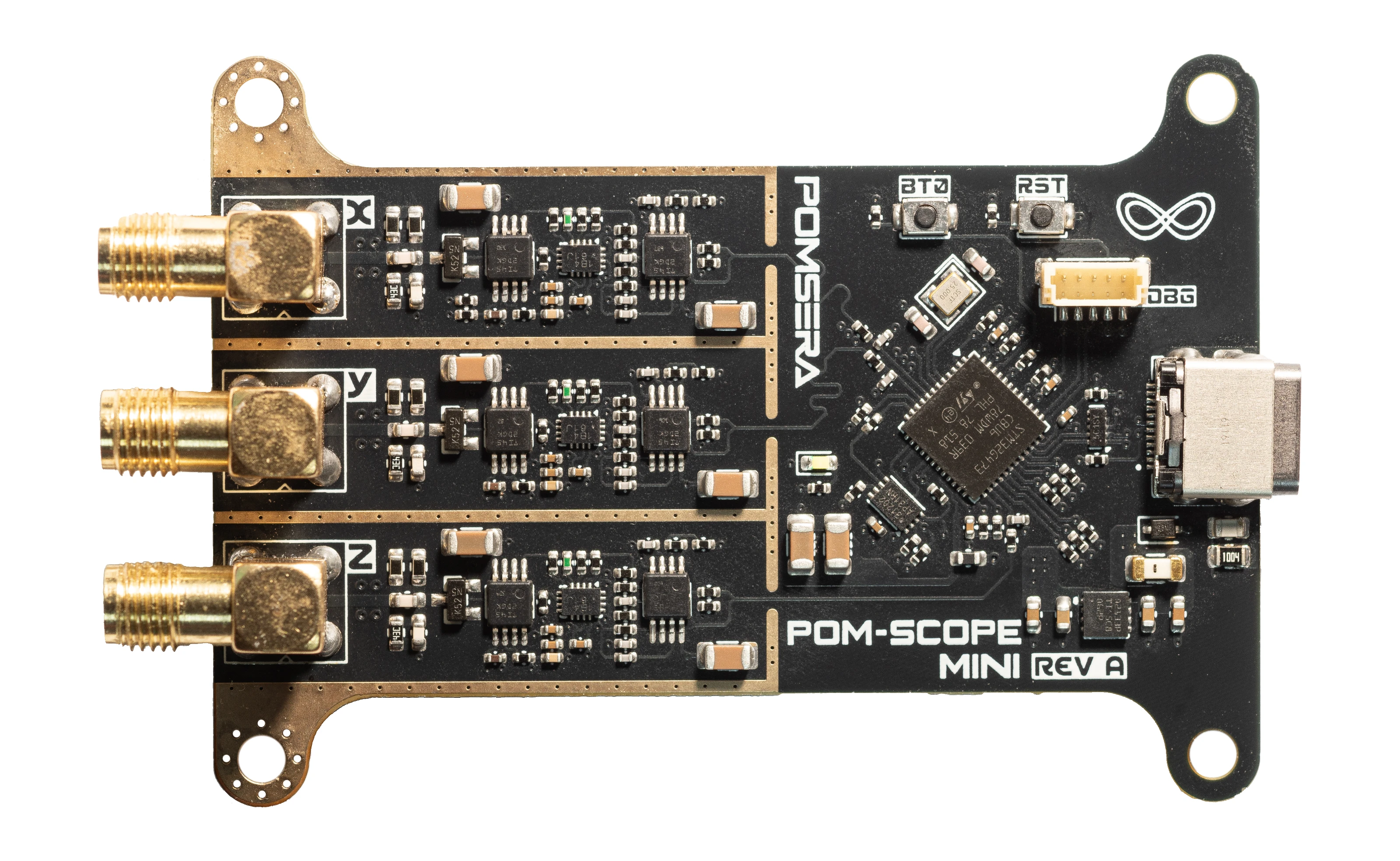
It is a compact, USB-powered oscilloscope with three synchronized analog channels, programmable input ranges and enough capture memory to record complete chaotic trajectories. Connect the three state variables of a Chua, Lorenz, Rössler or custom nonlinear circuit and the software can render XY projections or a rotatable XYZ point cloud in real time.
The target component cost is below $40 in small prototype quantities, excluding probes, shipping and taxes. It is not trying to replace a 100 MHz bench oscilloscope. It is a purpose-built instrument for low-frequency analog dynamics, where channel synchronization, resolution and capture depth matter more than headline bandwidth.
PomScope Mini has common-ground inputs connected to USB ground. It is intended for low-voltage, ground-referenced circuits. It must not be used directly on mains, offline power supplies or floating high-energy systems.
The problem with using a normal cheap oscilloscope
A two-channel oscilloscope can display an XY projection. That is enough to recognize a double scroll, but it is still only a shadow of the system.
For a three-state circuit, every sample is a point:
If the three voltages are not sampled at the same instant, the plotted point never truly existed. Multiplexing one ADC between three inputs introduces a time offset that bends fast trajectories. Using only two channels forces you to choose XY, XZ or YZ and lose the complete state.
PomScope Mini triggers three independent ADCs from the same timer. Each record therefore contains a synchronized X, Y and Z sample. That single decision is the reason the board makes sense.
PomScope Mini specifications
| Specification | PomScope Mini |
|---|---|
| Analog channels | 3 synchronized channels (12-bit native Resolution) |
| Live USB mode | Up to 200 kS/s per channel |
| Burst acquisition target | Up to 1.7 MS/s per channel |
| Analog filter | Fourth-order low-pass, approximately 250 kHz |
| Input impedance | Approximately 1 MΩ |
| Nominal input ranges | ±2.5 V, ±5 V, ±10 V and ±20 V |
| Capture memory | 8 MiB external PSRAM |
| Stored records | Approximately 1.39 million XYZ samples at 16-bit storage |
| Connection | USB-C, USB 2.0 Full Speed |
| Input connectors | 3 SMA |
| Display modes | Time, XY, XZ, YZ and rotatable XYZ point cloud |
| Input grounding | Common ground, non-isolated |
These numbers deliberately describe the complete instrument rather than quoting only the fastest peripheral inside the microcontroller.
Why the STM32G473 is at the centre
The STM32G473CBU6 combines a 170 MHz Cortex-M4, several fast 12-bit ADCs, DMA, USB Full Speed and a QSPI interface in a compact QFN package. ST rates the ADC blocks at up to 4 MSPS, but the system does not advertise 4 MS/s per channel: the analog bandwidth, memory path, USB transport and signal integrity must all work together.
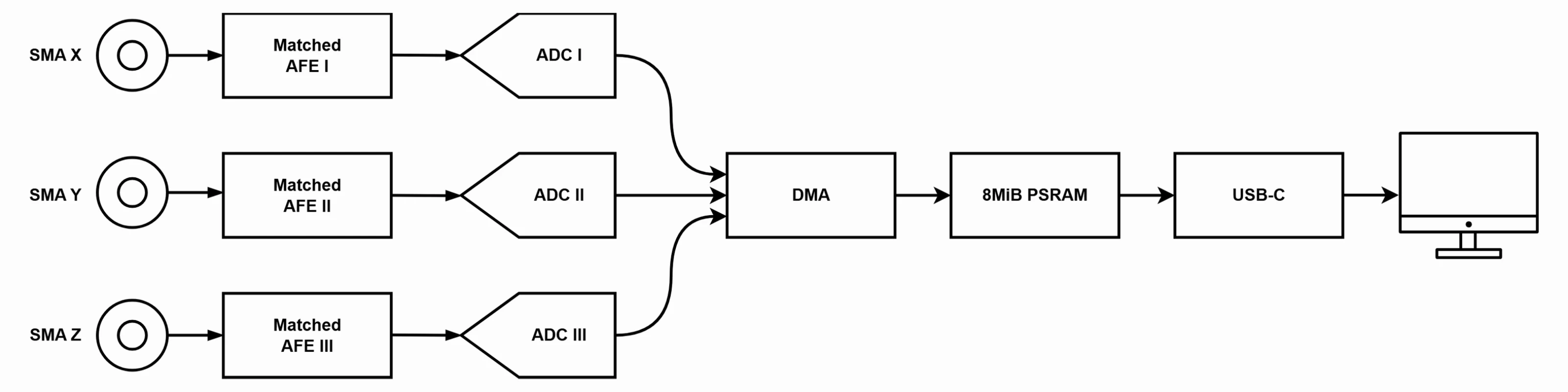
Three ADC instances are assigned to the three inputs and started by one hardware timer. All three ADC instances use a common clock configuration and a common hardware timer trigger, following ST's recommendations for concurrent ADC operation on the STM32G473. DMA moves the results without asking the CPU to service every sample. The processor can then handle triggering, gain control, framing, calibration and USB communication.
An FPGA or external simultaneous ADC could push the sampling rate much higher, but it would add cost, power rails, routing constraints and firmware complexity. For attractors whose useful spectrum sits below a few hundred kilohertz, the STM32G473 is the better engineering trade.
One analog front end, repeated three times
Each channel follows the same signal path:
SMA input → compensated attenuator → protection → programmable gain → fourth-order filter → ADC isolation network → STM32 ADC
1. High-impedance attenuation
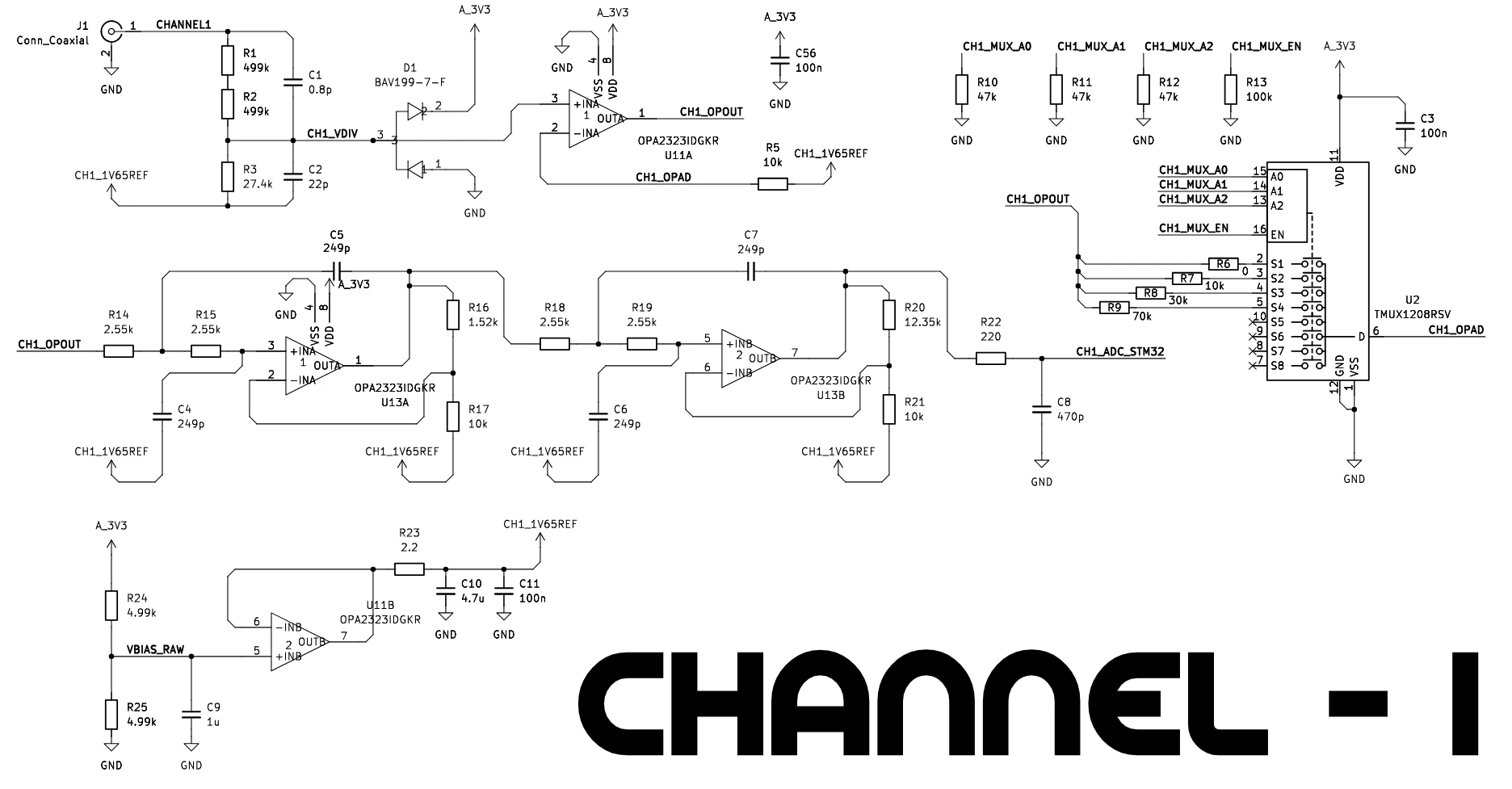
The input first sees two 499 kΩ resistors above a 27.4 kΩ lower leg. The resulting attenuation is approximately:
The input impedance remains close to 1 MΩ, so the scope does not heavily load the chaotic circuit. A 0.8 pF upper capacitor and 22 pF lower capacitor compensate the divider at higher frequencies. These values include an allowance for diode, amplifier and PCB parasitics and are finalized with square-wave calibration.
2. Protection and bias
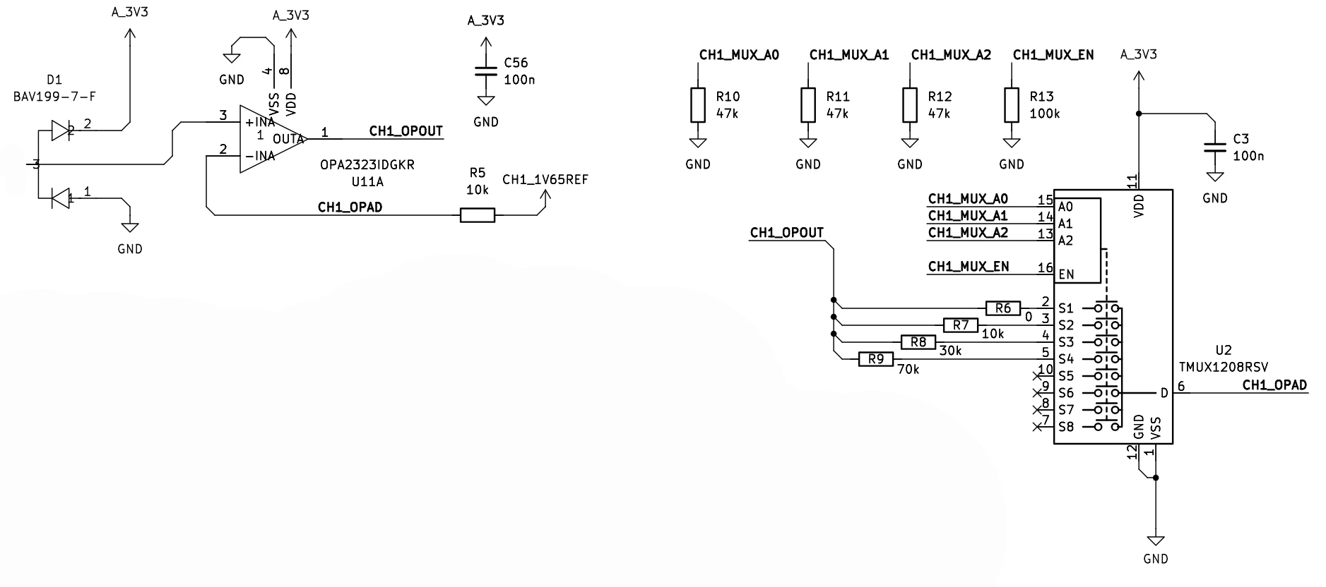
The attenuated node is protected by a low-leakage BAV199 clamp. The analog chain is centred around a quiet 1.65 V bias, allowing positive and negative input signals to fit inside the STM32's 0 to 3.3 V ADC range.
This bias is not ground. It is the local midpoint around which the AC signal moves.
3. Programmable gain
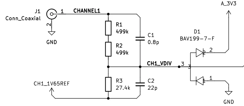
An OPA2323 and TMUX1208 select gains of ×1, ×2, ×4 or ×8. Combined with the attenuator and filter gain, this produces four useful nominal ranges:
| Selected gain | Nominal input range |
|---|---|
| ×1 | ±20 V |
| ×2 | ±10 V |
| ×4 | ±5 V |
| ×8 | ±2.5 V |
The smaller range is important. Measuring a 4 V peak-to-peak attractor on a fixed ±20 V input would waste most of the ADC codes.
4. Two second-order filters make one fourth-order filter
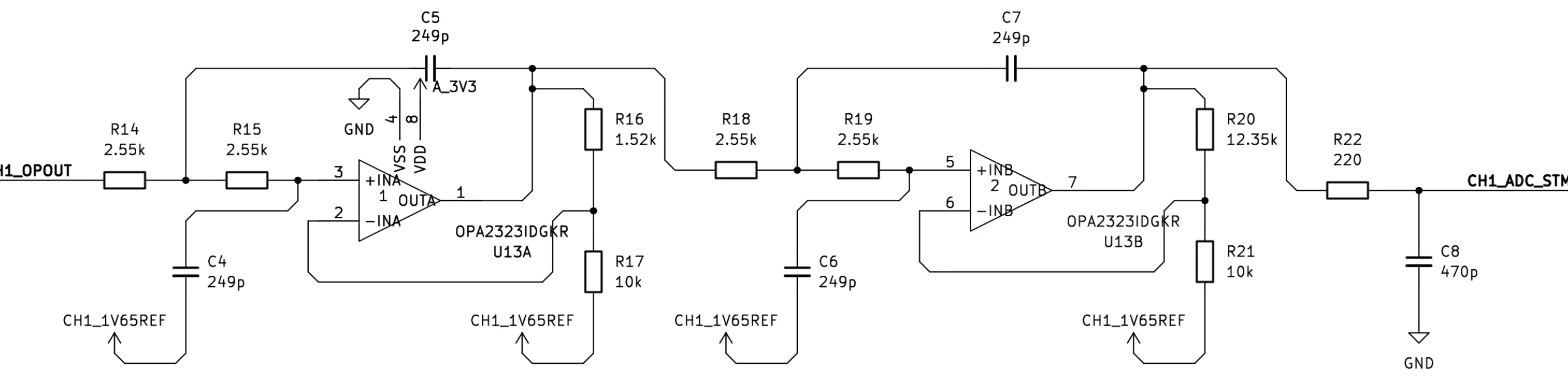
The anti-aliasing filter uses two Sallen-Key sections. Both use 2.55 kΩ resistors and 249 pF C0G capacitors, placing their natural frequency near 251 kHz. Their quality factors are intentionally different:
Together they form a fourth-order Butterworth response: flat through the useful band, followed by a much steeper rejection than one second-order stage could provide. The two sections have a combined AC gain of approximately 2.575, which is included in the input-range calculation.
The final 220 Ω and 470 pF network isolates the last amplifier from the STM32 sampling capacitor and absorbs the short current pulses produced when the ADC acquires a sample.
Why 8 MiB matters more than a huge bandwidth number
At 16-bit storage, one synchronized XYZ record occupies six bytes. The 8 MiB PSRAM can therefore hold roughly:
That is approximately 1.4 seconds at 1 MS/s per channel, 2.8 seconds at 500 kS/s or almost 14 seconds at 100 kS/s.
USB Full Speed cannot continuously carry three 1 MS/s, 16-bit streams. PomScope Mini therefore has two useful operating modes:
- Live mode: stream up to 200 kS/s per channel for responsive XY and XYZ visualization.
- Burst mode: capture faster data into PSRAM, stop, then transfer the complete record to the computer.
This is a better fit for chaotic circuits than reducing every acquisition to a tiny oscilloscope buffer.
Analog Front End - Simulation
Capturing a real Chua attractor in 3D
A scope designed for nonlinear systems should be tested on a physical nonlinear system, not only on a signal generator. For this validation, I connected PomScope Mini to a Chua oscillator and measured three circuit state variables at the same time. Each state variable was connected to one SMA input. The Chua circuit and PomScope Mini shared the same 0 V reference. Because all three STM32 ADCs are triggered by the same timer, every acquisition produces one synchronized three-dimensional record.
Why synchronization matters: if X, Y and Z came from different instants, the software could still draw an attractive-looking point cloud, but its geometry would no longer represent the real trajectory of the circuit.

Video available in the online article.
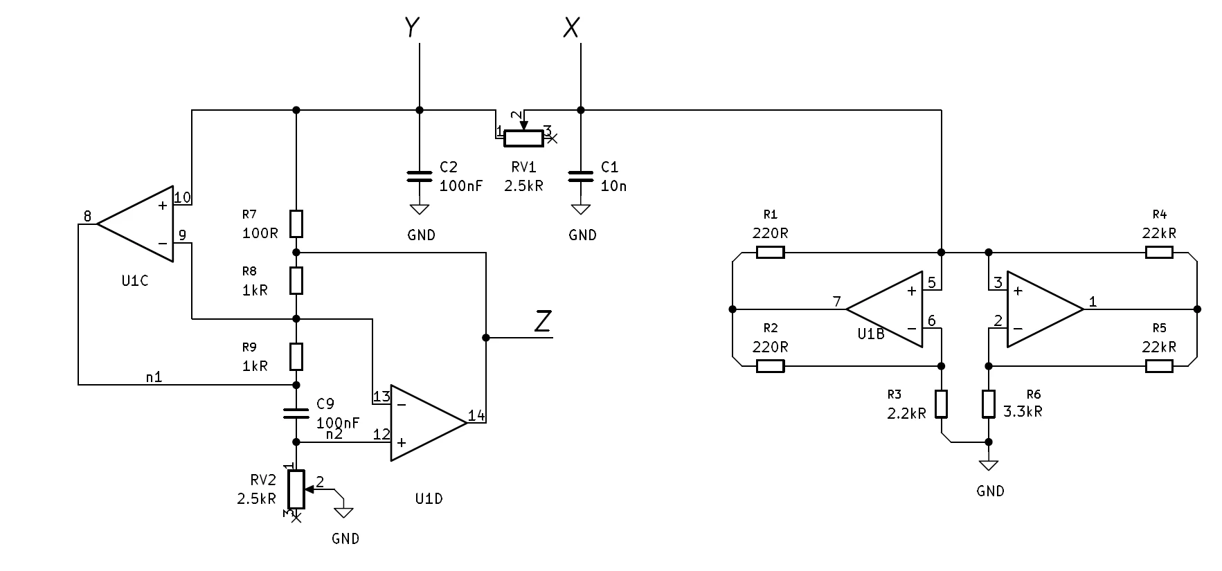
The video above was recorded using the simple op-amp Chua circuit shown here. Capacitors C1 and C2 provide the X and Y state voltages, while the active-inductor stage produces the third state, Z. The remaining op-amp network implements Chua's nonlinear negative resistance, and the two potentiometers tune the circuit into the double-scroll regime. These X, Y and Z test points are buffered and connected to the three PomScope Mini inputs.
Printed Circuit Board
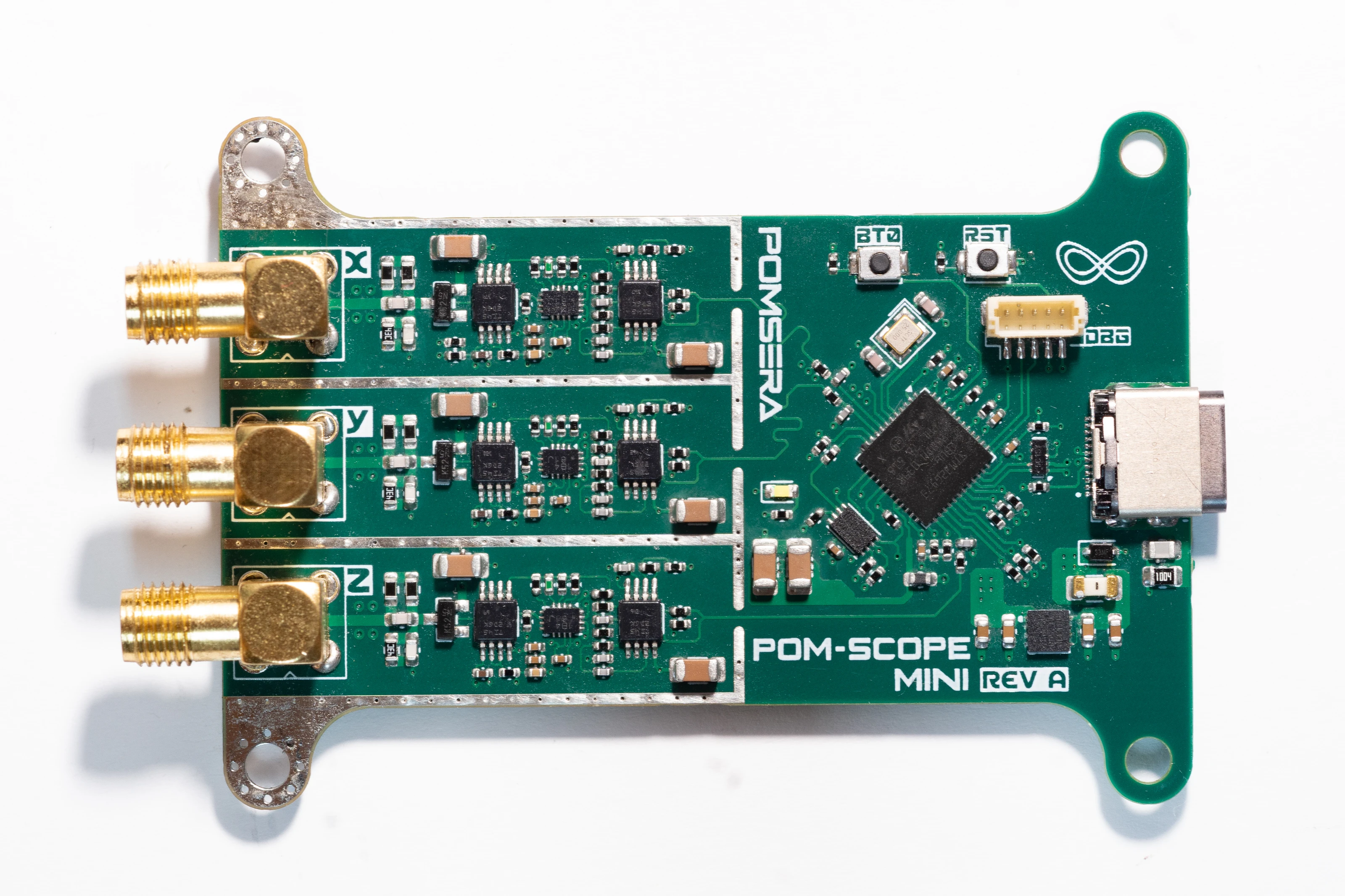
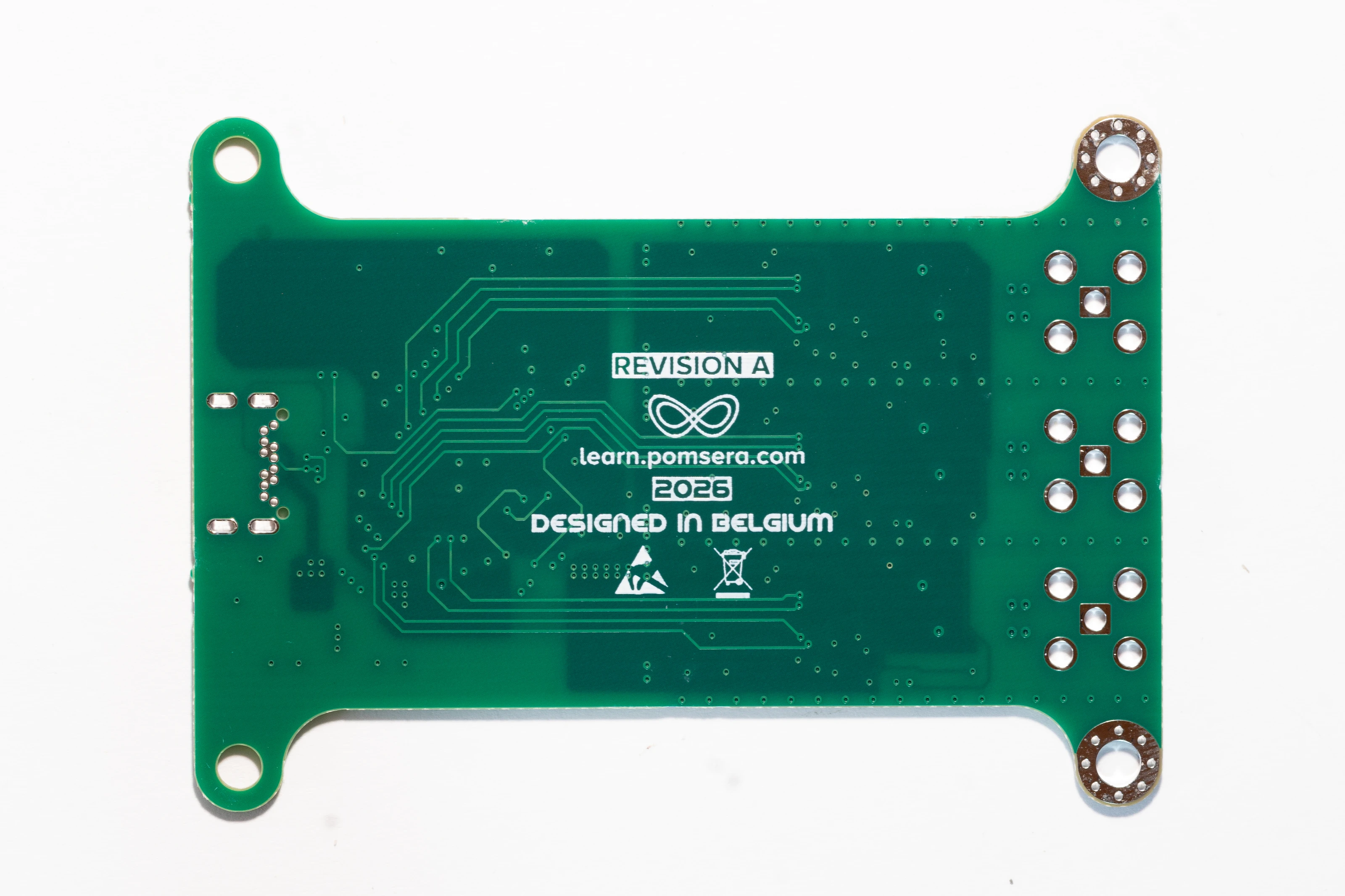
Schematic
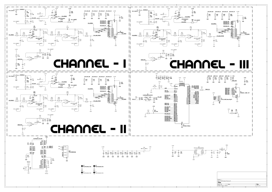
This article is primarily a hardware-oriented introduction to designing a simple analog front end for synchronized ADC acquisition. It focuses on the input attenuator, protection, programmable gain, filtering, biasing and ADC interface rather than documenting every part of PomScope Mini as a reproducible product. The schematic is provided to support that explanation, but the PCB source files, manufacturing package, firmware and desktop software are not published. Those elements are specific to the complete instrument and remain under active development, while the purpose of this article is to teach the analog design principles that can be reused in other measurement projects.